Product
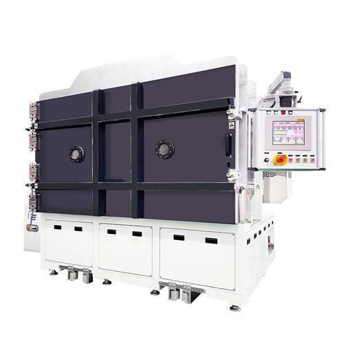
NEMST-HPE2018 系列
Microwave Plasma Etching Machine
- High efficiency microwave (MW) plasma source design: 1011~1013/cm3.
- Unique Distribution Panel Design is employed to ensure uHigh-efficiency uniform plasma generation.
- No Damage on substrate/product By employing Filtered Plasma Design.
- Unique ECR (Electron Cyclotron Resonator) Design to create high-density plasma and extend the lifetime of isolation quartz plate.
- Large-area panel treatment is available.
- High Etching Rate (1~10 um / min in general.
- Very high treatment uniformity. (Up to 90%)
- Low Temperature Treatment is available. (≦ 120 ℃)
- Damage Free on the products.
- Large Area Treatment is available (e.g. 500 mm x 600 mm)
- Suitable for etching Polymer Material (Polyimide, Parylene, FR4, BT, Teflon, etc.), Silicon, Passivation (Si3N4 or SiON), Dielectric (SiO2, High-K, Low-K, etc.), Semiconductor Compound (GaN, GaAs, InP, SiC and etc), Metals (Al, Ti, Metal Alloys and etc), Other Material (Sapphire, Diamond, ITO, PZT, etc.).
- Employed for Processes of Semiconductor, Advanced Packaging (Wafer-Level Packaging, Panel-Level Packaging, 2.5D/3D, CoWoS), IC Substrate, Mirco-LED, Wafer Reclaim, and etc.